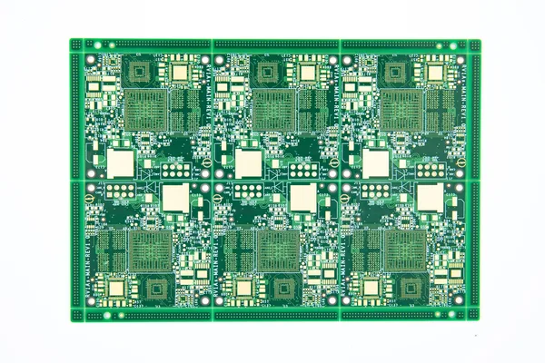
The circuit board determines the process difficulty and processing price according to the number of wiring surfaces. Ordinary circuit boards are divided into single-sided wiring and double-sided wiring, commonly known as single-sided and double-sided. However, high-end electronic products are restricted by product space design factors. Outside the surface wiring, multiple layers of circuits can be superimposed on the inside. During the production process, after each layer of circuits is fabricated, they are positioned and pressed together by optical equipment, so that the multi-layer circuits are superimposed on a circuit board, which is a multilayer PCB. Any circuit board with more than or equal to 2 layers can be called a multilayer PCB. Multilayer PCB can be divided into multi-layer rigid circuit boards, multi-layer flexible and rigid circuit boards and multi-layer flexible and rigid circuit boards.

In the layout of the printed circuit, unforeseen design problems such as noise, stray capacitance, crosstalk, etc. appear. Therefore, printed circuit board design must focus on minimizing signal line lengths and avoiding parallel routes. Obviously, these questions cannot be answered satisfactorily in single-panel, or even double-panel, due to the limited number of crossovers that can be achieved. In the case of a large number of interconnection and crossover requirements, in order to achieve a satisfactory performance of the circuit board, the board layer must be expanded to more than two layers, thus the emergence of the multilayer PCB. Therefore, the original intention of making a multilayer PCB is to provide more degrees of freedom in choosing suitable routing paths for complex and/or noise-sensitive electronic circuits. A multilayer PCB has at least three conductive layers, two of which are on the outer surface, and the remaining one is synthesized inside the insulating board. The electrical connection between them is usually achieved through plated through holes in the cross section of the circuit board.
The use of multilayer PCB is in professional electronic equipment (computers, military equipment), especially in the case of overloaded weight and volume. However, this can only be an increase in the cost of multiple substrates in exchange for an increase in space and a reduction in weight. In high-speed circuits, multiple substrates are also very useful, they can provide the designer of the printed circuit board with more than two layers of the board surface to route the wires and provide large ground and power areas.

Email: sales@fastlinkpcb.com
Phone: +86 - 0755- 23597570
Tel: +86 15171508318
Head office: 3A12 ,Floor 4, JinYuan Building B , Xixiang Rd, Bao'an district, ShenZhen , China
Factory Address: 3rd floor, Building D, Baishixia Industrial Zone, Jian 'an Road, Fuhai Street, Bao 'an District, Shenzhen ,china
After I initially left a comment I seem to have clicked the -Notify me when new comments are added- checkbox and from now on each time a comment is added I get four emails with the exact same comment. Perhaps there is a means you are able to remove me from that service? Thanks!
Greetings! Very useful advice in this particular article! Its the little changes that will make the biggest changes. Thanks for sharing!
Good post. I learn something totally new and challenging on blogs I stumbleupon on a daily basis. Its always useful to read content from other authors and practice something from their websites.