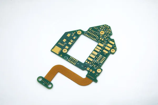
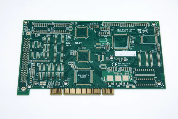
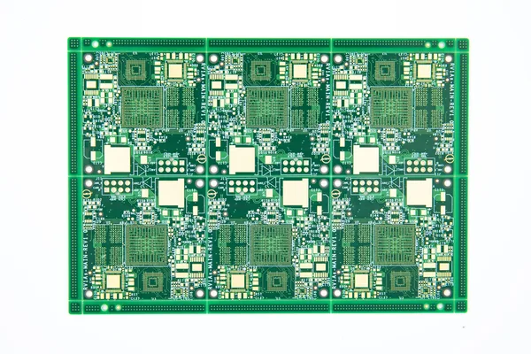
High-frequency PCB refers to a special circuit board with high electromagnetic frequency, which is used for PCB in the fields of high frequency (frequency greater than 300MHZ or wavelength less than 1 meter) and microwave (frequency greater than 3GHZ or wavelength less than 0.1 meters). The copper plate is a circuit board produced by using part of the process of the ordinary rigid circuit board manufacturing method or using a special treatment method.

In high-frequency circuit design, the power supply is designed in the form of layers, which in most cases is much better than the form of buses, so that the loop can always follow the path of least impedance. In addition, the power board must provide a signal loop for all signals generated and received on the PCB, which can minimize the signal loop, thereby reducing noise, which is often overlooked by low-frequency circuit designers.
In high frequency PCB design, we should follow the following principles:
1. The unity and stability of power supply and ground;
2. Careful wiring and proper termination can eliminate reflections;
3. Careful wiring and proper termination can reduce capacitive and inductive crosstalk;
4. Noise suppression is required to meet EMC requirements.
1. The dielectric loss must be small, which mainly affects the quality of signal transmission. The smaller the dielectric loss, the smaller the signal loss.
2. Low water absorption and high water absorption will affect the dielectric constant and dielectric loss when wet.
3. The dielectric constant must be small and stable. Usually, the smaller the better, the signal transmission rate is inversely proportional to the square root of the dielectric constant of the material. High dielectric constant is likely to cause signal transmission delay.
4. The thermal expansion coefficient of the copper foil should be as consistent as possible, because the inconsistency will cause the copper foil to separate in the hot and cold changes.
5. Other heat resistance, chemical resistance, impact strength, peel strength, etc. must also be good.
Flex PCB is a highly reliable and excellent flexible printed circuit board made of polyimide or polyester film. It has the characteristics of high wiring density, light weight, thin thickness and good bendability. Flexible circuit is a technology developed by the United States for the development of aerospace rocket technology in the 1970s. It is a highly reliable and extremely flexible printed circuit made of polyester film or polyimide as the base material. By embedding a circuit design on a flexible thin plastic sheet, a large number of precision components can be stacked in a narrow and limited space, thereby forming a flexible flexible circuit. This kind of circuit can be bent and folded at will, light weight, small size, good heat dissipation, convenient installation, breaking through the traditional interconnection technology. In the structure of flexible circuits, the constituent materials are insulating films, conductors and adhesives.

Rigid PCB and flex PCB have both similarities and differences at the same time. For flex PCBs, rigid PCBs are more widely used. Because rigid PCBs appeared earlier, most of the design elements of rigid PCBs have been applied to the design of flex PCBs. So what are the differences between rigid PCBs and flex PCBs?
1. The current carrying capacity of the wire: Compared with the rigid PCB, the heat dissipation performance of the flex PCB is relatively poor, so sufficient wire width must be provided. Due to the heat dissipation problem of the flex PCB, it is necessary to give extra width or spacing to the wires.
2. Shape: In general, a rectangle is selected, which can save the substrate very well, and there should be enough free margins near the edge. A sharp inner corner may cause tearing of the board. Therefore, the smaller wire width and spacing should be minimized as much as possible, and the transition must be as smooth as possible. Sharp corners will naturally concentrate stress and cause wire failure.
3. Flexibility: The flexibility of rigid PCB is of course not comparable to that of flex PCB. For a large number of bending cycles, flex PCB has better performance.
Printed circuit boards can be divided into rigid PCBs and flexible printed boards according to the production materials. rigid PCB has phenolic paper laminate, epoxy paper laminate, polyester glass felt laminate, epoxy glass cloth laminate. Common thicknesses of rigid PCBs are 0.2mm, 0.4mm, 0.6mm, 0.8mm, 1.0mm, 1.2mm, 1.6mm, 2.0mm, etc.

Rigid circuit boards have the following characteristics:
1. High density: For more than 100 years, the high density of printed boards can be developed with the improvement of integrated circuit integration and the advancement of installation technology.
2. High reliability: Through a series of inspections, tests and aging tests, the PCB can be guaranteed to work reliably for a long time (usage period, generally 20 years).
3. Designability: For various performance requirements of PCB (electrical, physical, chemical, mechanical, etc.), PCB design can be realized through design standardization and standardization, with short time and high efficiency.
4. Productivity: With modern management, standardization, scale (quantification), automation and other production can be carried out to ensure the consistency of product quality.
5. Testability: Establish relatively complete test methods, test standards, various test equipment and instruments, etc. to detect and identify the qualification and service life of PCB products.
After the electronic equipment adopts the printed board, due to the consistency of the same type of printed board, the error of manual wiring is avoided, and the automatic insertion or mounting of electronic components, automatic soldering, and automatic detection can be realized, which ensures the quality of the electronic equipment. , improve labor productivity, reduce costs, and facilitate maintenance.
A summary of the development trends of future printed board manufacturing technology at home and abroad is basically the same, that is, to high density, high precision, fine aperture, fine wire, fine pitch, high reliability, multi-layer, high-speed transmission, light weight, and thin direction of development.
The circuit board determines the process difficulty and processing price according to the number of wiring surfaces. Ordinary circuit boards are divided into single-sided wiring and double-sided wiring, commonly known as single-sided and double-sided. However, high-end electronic products are restricted by product space design factors. Outside the surface wiring, multiple layers of circuits can be superimposed on the inside. During the production process, after each layer of circuits is fabricated, they are positioned and pressed together by optical equipment, so that the multi-layer circuits are superimposed on a circuit board, which is a multilayer PCB. Any circuit board with more than or equal to 2 layers can be called a multilayer PCB. Multilayer PCB can be divided into multi-layer rigid circuit boards, multi-layer flexible and rigid circuit boards and multi-layer flexible and rigid circuit boards.

In the layout of the printed circuit, unforeseen design problems such as noise, stray capacitance, crosstalk, etc. appear. Therefore, printed circuit board design must focus on minimizing signal line lengths and avoiding parallel routes. Obviously, these questions cannot be answered satisfactorily in single-panel, or even double-panel, due to the limited number of crossovers that can be achieved. In the case of a large number of interconnection and crossover requirements, in order to achieve a satisfactory performance of the circuit board, the board layer must be expanded to more than two layers, thus the emergence of the multilayer PCB. Therefore, the original intention of making a multilayer PCB is to provide more degrees of freedom in choosing suitable routing paths for complex and/or noise-sensitive electronic circuits. A multilayer PCB has at least three conductive layers, two of which are on the outer surface, and the remaining one is synthesized inside the insulating board. The electrical connection between them is usually achieved through plated through holes in the cross section of the circuit board.
The use of multilayer PCB is in professional electronic equipment (computers, military equipment), especially in the case of overloaded weight and volume. However, this can only be an increase in the cost of multiple substrates in exchange for an increase in space and a reduction in weight. In high-speed circuits, multiple substrates are also very useful, they can provide the designer of the printed circuit board with more than two layers of the board surface to route the wires and provide large ground and power areas.

Email: sales@fastlinkpcb.com
Phone: +86 - 0755- 23597570
Tel: +86 15171508318
Head office: 3A12 ,Floor 4, JinYuan Building B , Xixiang Rd, Bao'an district, ShenZhen , China
Factory Address: 3rd floor, Building D, Baishixia Industrial Zone, Jian 'an Road, Fuhai Street, Bao 'an District, Shenzhen ,china