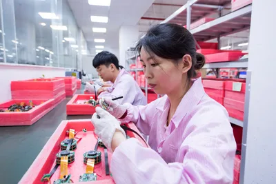
With the development of electronic product PCB assembly towards miniaturization and high assembly density, SMT surface mount technology has now become the mainstream technology of electronic assembly. However, due to the large size of some electronic components in PCB assembly and processing, plug-in processing has not been replaced, and still plays an important role in the electronic assembly process, so there will be a certain number of through-hole plug-in in the PCB circuit board. components. The assembly of both plug-in components and surface mount components is called hybrid assembly, referred to as mixed assembly, and the assembly of all surface mount components is called full surface mount.

The PCB assembly method and its technological process mainly depend on the type of assembled components and the equipment conditions of the assembly. What are the steps involved in PCB Assembly?
1. Application of solder paste: Before adding components, solder paste needs to be added, and the solder paste needs to be added to the area of the circuit board to be coated with solder.
2. Placing components: Placing components is done after applying solder paste. Surface mount technology requires precise placement of components, which is difficult to achieve with manual placement. Therefore, a pick and place machine is required to place the components on the circuit board.
3. Reflow oven: In this step, the actual connection takes place. After the components are placed, the board is placed on a reflow oven conveyor, and the solder applied during the soldering process melts during reflow, which permanently connects the component to the board.
4. Wave Soldering: In this step, printed circuit boards are placed on a system driven by a mechanical conveyor and passed through different areas. The PCB passes through a molten solder wave, which helps connect the PCB pads/holes, electronic component leads and solder.
5. Cleaning the PCB: It is very important to clean the PCB after assembly, this process helps to clean all flux residues with the help of ionized water.
6. Check the PCB assembly: This is one of the most important steps in PCB assembly. During this step, check the board for shorts, loose solder balls, and bridges between solder balls.
7. Test the board and monitor the output: This is the last step in the process. This step involves monitoring whether the product provides the desired output.

Email: sales@fastlinkpcb.com
Phone: +86 - 0755- 23597570
Tel: +86 15171508318
Head office: 3A12 ,Floor 4, JinYuan Building B , Xixiang Rd, Bao'an district, ShenZhen , China
Factory Address: 3rd floor, Building D, Baishixia Industrial Zone, Jian 'an Road, Fuhai Street, Bao 'an District, Shenzhen ,china
Greetings! Very useful advice in this particular article! Its the little changes that will make the biggest changes. Thanks for sharing!
Great article! I found your perspective on this topic both enlightening and thought-provoking. The way you break down complex ideas into understandable insights is truly commendable. It’s interesting to see how these developments could shape our future. I’m particularly intrigued by your point about potential challenges and would love to dive deeper into that.
For those who are interested in exploring this topic further, I recommend checking out this resource for more detailed information: comprehensive guide. It offers additional insights that complement what’s discussed here.
Looking forward to hearing others’ thoughts and continuing this discussion. Thanks for sharing such valuable information!
Great article! I appreciate the clear and insightful perspective you’ve shared. It’s fascinating to see how this topic is developing. For those interested in diving deeper, I found an excellent resource that expands on these ideas: check it out here. Looking forward to hearing others’ thoughts and continuing the discussion!
The arguments in this article were very well-presented. I appreciate the depth of analysis. It would be interesting to hear how others interpret these points. What do you think?